Shenzhen Tengxingsheng Electronics Co., Ltd.
Contact: Miss Wen
Tel: 0755-23286182
Mob: 13570819121
QQ: 1456258664
QQ: 2316907424
Fax: 0755-23286183
Email: txspcbsc@163.com txspcb@163.com
Web : en.txspcb.cn
Add: 3rd Floor, Building 3, Jinkang Industrial Park, No. 1 Shajing Road, Baoan District, Shenzhen
How much do you know about several important steps in pcb circuit board design?
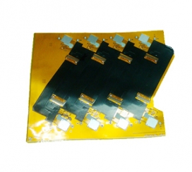
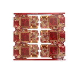
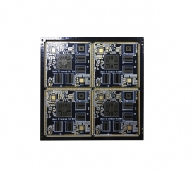
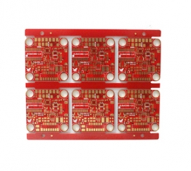
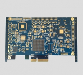
PCB circuit board is one of the most important components in the electronics industry, and almost every electronic device needs to use it. Its design can not only directly affect the quality of the entire electronic product, but also is closely related to the cost, and can even control the success or failure of business competition. It is not easy to say, but it is not difficult to say that it is difficult. Just follow these steps, and you can easily complete thePCB circuit boarddesign.
1. Pay attention to the relationship between vias, pads, traces and gold fingers
During wiring, the vias should not be too close to the pads, traces, and gold fingers. The vias of the same attribute should be kept at least 0.12mm away from the gold fingers, and the vias of different attributes should be kept away from the pads and the gold fingers. The via hole should be as small as possible to make the outer hole 0.35mm and the inner hole 0.2mm.
2. Pay attention to the distance between the pad and the original
The distance between the SMT pad and the DIE bonding pad and SMT components should be kept more than 0.3mm, and the distance between one DIE bonding pad and another DIE should also be kept more than 0.2mm. The minimum signal trace is 2MILS, the spacing is 2MILS, and the main power trace is preferably 6-8MILS to enhance the strength of the substrate.
3. Pay attention to the size and spacing of the pads
The minimum size of the bonding pad (single wire) is 0.2mmX0.09mm90 degrees, the spacing between the pads is as small as 2MILS, and the width of the ground and power lines in the inner row is also required to be 0.2mm. At the same time, the angle of the bonding pad should be adjusted according to the angle of the component cable.
4. Pay attention to the manufacturing process of the substrate
Each line must be poured with copper material by electroplating method to form pads and traces. Even if there is no network pad, the pad must be copper-plated in a certain mode, otherwise this will appear. The result is that the pads are copper-free.

Mob: 13570819121
Email: txspcbsc@163.com
Web : www.txspcb.cn
Add: Jinkang, No. 1 Shajing Road, Baoan District, Shenzhen
3rd Floor, Building 3, Industrial Park

SWEEP
 Online Service


 中文
中文 English