Shenzhen Tengxingsheng Electronics Co., Ltd.
Contact: Miss Wen
Tel: 0755-23286182
Mob: 13570819121
QQ: 1456258664
QQ: 2316907424
Fax: 0755-23286183
Email: txspcbsc@163.com txspcb@163.com
Web : en.txspcb.cn
Add: 3rd Floor, Building 3, Jinkang Industrial Park, No. 1 Shajing Road, Baoan District, Shenzhen
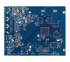
We all know that doingWhen designing the PCB circuit board , if it is only a general board, it is only necessary to do the precise design of the mechanical size. However, if you encounter high-frequency signals, use load lines or long lines, etc., you must deal with these lines specially. Otherwise, it is very likely to cause reflection, crosstalk between lines, and a series of signal interference. question. Therefore, when we are doing circuit design, especially when we are doing high-speed PCB design, we must do a good job of anti-interference of line signals, and shielding methods are often necessary to correct errors. The following editor will tell you about the PCB circuit board wiring and how to do the electromagnetic compatibility design?
1. Appropriate wire width
When selecting the width of the wire, it should not only ensure the electrical function but also be convenient for production, which is usually determined by the minimum current value it can withstand. In order to reduce the electromagnetic interference impact of transient current on the printed board, it is necessary to control the line width in the design. Transient interference is generally caused by the inductance of the wire, which is proportional to the length of the wire and inversely proportional to the width of the wire. For signal lines that often have large transient currents, short and wide wires should be used. If the layout space allows, the well-shaped mesh layout should be used as much as possible.
2. The key to the wiring of components
Component wiring design mainly considers several aspects: First, the electrical function; when wiring, we try to put together the equipment that is closer to the connection, the layout of the high-speed line is as short as possible, and the power equipment and small signal equipment are as short as possible. To separate layout. The second is the orientation of the placement; whether the design is beautiful and regular, whether it is convenient for functional testing, later interface, and connection use. In the high-speed system, the transmission delay of the grounding and interconnecting lines is also a design factor that we need to consider first. The transmission time of the signal transmission line has a great influence on the overall system speed of the circuit. The general interconnection line will bring about the increase of delay time, which will greatly reduce the system speed.
3. Wiring rules for high-frequency and high-speed signals
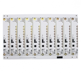
Usually, equal wiring can reduce the inductance between the wires, but in order to suppress the crosstalk of the PCB circuit wires, we should try to avoid long-distance equal wiring when designing the wiring; when designing the printed wires, avoid rapid turns and try to design them as It has a uniform curve with a certain radian; components with large currents on the circuit should be grounded separately to prevent noise interference, and grounding should be set between small signal or sensitive signal lines; high-speed signals use differential signal wiring design, Keeping the two differential lines in a positive and negative pair always keeps the transmission lines coupled to each other, effectively reducing the effects of electrical noise on the signal.Double-sided circuit board
Mob: 13570819121
Email: txspcbsc@163.com
Web : www.txspcb.cn
Add: Jinkang, No. 1 Shajing Road, Baoan District, Shenzhen
3rd Floor, Building 3, Industrial Park

SWEEP
 Online Service


 中文
中文 English