Shenzhen Tengxingsheng Electronics Co., Ltd.
Contact: Miss Wen
Tel: 0755-23286182
Mob: 13570819121
QQ: 1456258664
QQ: 2316907424
Fax: 0755-23286183
Email: txspcbsc@163.com txspcb@163.com
Web : en.txspcb.cn
Add: 3rd Floor, Building 3, Jinkang Industrial Park, No. 1 Shajing Road, Baoan District, Shenzhen
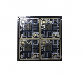
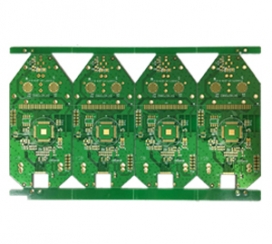
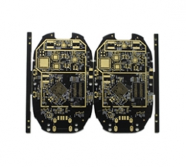
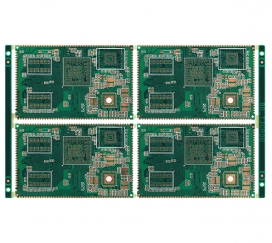
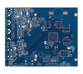
High-precision multi-layer PCB circuit board processing
With the development of modern electronic technology and the high speed and integration of chips, the electromagnetic environment inside and outside various electronic equipment systems is more complex, so multi-layer PCB processing is particularly important. Compared with single-sided boards , double-sided boards require higher technology and processing technology. It is multi-layer lamination, high-quality multi-layer PCB processing. Multilayer PCB, precision multi-layer circuit board production, Tengxingsheng Electronics Co., Ltd. A full set of imported automatic production lines, with its own various surface treatment equipment. In fact , the overall price of the multi -layer board must also be based on the basis of the multi-layer board proofing. Only when the samples are qualified, the product can be mass-produced; if the product size is relatively large, it can be satisfied. In the whole process of multi-layer board proofing, it is necessary to ensure that each revision meets the conditions and requirements, otherwise the inventory can only be treated as scrap, which is really a very painful realization.
1. Impedance characteristics of printed circuit boards
According to the theory of signal transmission, the signal is a function of time and distance variables, so each part of the signal may change on the connection. Therefore, the AC impedance of the connection is determined, that is, the ratio of the voltage change and the current change is the characteristic impedance of the transmission line (Characteristic Impedance): the characteristic impedance of the transmission line is only related to the characteristics of the signal connection itself. In the actual circuit, the resistance value of the wire itself is less than the distributed impedance of the system, just like in a high-frequency circuit, the characteristic impedance mainly depends on the distributed impedance brought by the unit distributed capacitance and unit distributed inductance of the connection. The characteristic impedance of an ideal transmission line depends only on the unit distributed capacitance and unit distributed inductance of the connection.
2. Calculation of characteristic impedance of printed circuit board
The proportional relationship between the rising edge time of the signal and the time it takes for the signal to transmit to the receiving end determines whether the signal connection is regarded as a transmission line. The specific proportional relationship can be explained by the following formula: If the length of the wire connection on the PCB is greater than l/b, the connection wire between the signals can be regarded as a transmission line. From the calculation formula of the signal equivalent impedance, the impedance of the transmission line can be expressed by the following formula: In the case of high frequency (tens of megahertz to hundreds of megahertz), wL>>R is satisfied (of course, in the range of signal frequency greater than 109Hz, then Considering the skin effect of the signal, this relationship needs to be carefully studied). Then for a certain transmission line, its characteristic impedance is a constant. The reflection phenomenon of the signal is caused by the inconsistency between the characteristic impedance of the driving end of the signal, the characteristic impedance of the transmission line and the impedance of the receiving end. For a CMOS circuit, the output impedance of the driving end of the signal is relatively small, tens of ohms. The input impedance of the receiving end is relatively large.
3. Characteristic impedance control of printed circuit boards
The characteristic impedance of the wires on the printed circuit board is an important indicator of circuit design. Especially in the PCB design of high-frequency circuits, it is necessary to consider whether the characteristic impedance of the wires is consistent with the characteristic impedance required by the device or signal, and whether it matches. Therefore, there are two concepts that must be paid attention to in the reliability design of PCB design.
4. Printed circuit board impedance control
There will be various signal transmissions in the conductors in the circuit board. When the frequency must be increased in order to increase the transmission rate, if the circuit itself is different due to factors such as etching, stack thickness, wire width, etc., the impedance value will change, making it Signal distortion. Therefore, the impedance value of the conductor on the high-speed circuit board should be controlled within a certain range, which is called "impedance control". The main factors that affect the impedance of PCB traces are the width of the copper wire, the thickness of the copper wire, the dielectric constant of the medium, the thickness of the medium, the thickness of the pad, the path of the ground wire, and the traces around the trace. Therefore, when designing the PCB, it is necessary to control the impedance of the wiring on the board, so as to avoid signal reflection and other electromagnetic interference and signal integrity problems as much as possible, and ensure the stability of the actual use of the PCB board. The calculation method of microstrip line and strip line impedance on the PCB board can refer to the corresponding empirical formula.

Mob: 13570819121
Email: txspcbsc@163.com
Web : www.txspcb.cn
Add: Jinkang, No. 1 Shajing Road, Baoan District, Shenzhen
3rd Floor, Building 3, Industrial Park

SWEEP
 Online Service


 中文
中文 English