Shenzhen Tengxingsheng Electronics Co., Ltd.
Contact: Miss Wen
Tel: 0755-23286182
Mob: 13570819121
QQ: 1456258664
QQ: 2316907424
Fax: 0755-23286183
Email: txspcbsc@163.com txspcb@163.com
Web : en.txspcb.cn
Add: 3rd Floor, Building 3, Jinkang Industrial Park, No. 1 Shajing Road, Baoan District, Shenzhen
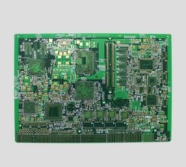
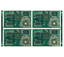
There are single-sided, double-sided and multi- layer PCB boards . The number of layers of a multi-layer board is not limited. At present, there are 100 multi-layer PCBs, and common multi-layer PCBs have four-layer and six-layer boards. So why do people have the question of "why are all even-numbered layers of PCB multilayer boards"? Relatively speaking, even-layer PCBs do have advantages over odd-layer PCBs.
1. Low cost
Odd-numbered PCBs have slightly lower raw material costs than even-numbered PCBs due to one less dielectric and foil layer. However, the processing cost of odd-layer PCBs is significantly higher than even-layer PCBs. The processing cost of the inner layer is the same, but the foil/core structure significantly increases the processing cost of the outer layer.
Odd-layer PCBs require a non-standard laminated core layer bonding process based on the core structure process. Factories that add foil outside the core structure will lose productivity compared to the core structure. The outer core requires additional processing prior to lamination bonding, which increases the risk of scratching and etching errors on the outer layer.

2. Balanced structure to avoid bending
The best reason not to design an odd-layer PCB is that odd-layer boards are prone to flexing. When the PCB is cooled after the multilayer circuit bonding process, the different lamination tensions of the core structure and the cladding structure as they cool can cause the PCB to bend. As the thickness of the board increases, the risk of bending a composite PCB with two different structures increases. The key to eliminating board flex is balanced stacking. Although a PCB with a certain curvature meets the requirements of the specification, it will reduce the efficiency of subsequent processing and increase the cost. Quality suffers because assembly requires special equipment and processes that reduce the accuracy of component placement.
In other words, it is easier to understand: in the PCB process, the four -layer board is easier to control than the three-layer board, mainly in terms of symmetry, the warpage of the four-layer board can be controlled below 0.7% (IPC600 standard), but when When the size of the three-layer board is large, the warpage will exceed this standard, affecting the reliability of the SMT patch and the entire product. Therefore, ordinary designers do not design odd layers. Even if the odd-numbered layers implement functions, they will be designed as pseudo-even-numbered layers, that is, 5 layers are designed to be 6 layers, and 7 layers are designed to be 8 layers.
For the above reasons, most of the PCB multilayer boards are designed with even layers and fewer odd layers.
How to balance the stackup and reduce the cost of odd-numbered PCBs?
What if the design has an odd number of layers of PCB? The following methods can be used to achieve balanced stacking, reduce PCB manufacturing costs, and avoid PCB bending.

1) A signal layer and its purpose. This method can be used if the design PCB has an even number of power planes and an odd number of signal planes. The increased number of layers does not increase cost, but can shorten lead times and improve PCB quality.
2) Add an extra power plane. This method can be used if the design PCB has an odd number of power planes and an even number of signal planes. An easy way to do this is to add a formation in the middle of the stack without changing other settings. First, route the PCB on odd layers, then duplicate the ground layer in the middle, and mark the remaining layers. This is the same as the electrical properties of the thickened layer foil.
3) Add a blank signal layer near the center of the PCB stackup. This approach minimizes stack imbalance and improves PCB quality. Route the odd layers first, then add blank signal layers and label the rest. It is used in microwave circuits and mixed-medium (mediums with different dielectric constants) circuits.
Mob: 13570819121
Email: txspcbsc@163.com
Web : www.txspcb.cn
Add: Jinkang, No. 1 Shajing Road, Baoan District, Shenzhen
3rd Floor, Building 3, Industrial Park

SWEEP
 Online Service


 中文
中文 English