Shenzhen Tengxingsheng Electronics Co., Ltd.
Contact: Miss Wen
Tel: 0755-23286182
Mob: 13570819121
QQ: 1456258664
QQ: 2316907424
Fax: 0755-23286183
Email: txspcbsc@163.com txspcb@163.com
Web : en.txspcb.cn
Add: 3rd Floor, Building 3, Jinkang Industrial Park, No. 1 Shajing Road, Baoan District, Shenzhen
The pcb is made of different components and a variety of complex process technologies, among which the structure of the pcb circuit board has a single-layer, double-layer, and multi-layer structure, and the production methods of different hierarchical structures are different. This article will introduce in detail: the component names and corresponding uses of pcb circuit boards, the production of single-layer, double-layer, and multi-layer structures of pcb circuit boards, and the main functions of various types of working layers.
First, the printed circuit board is mainly composed of pads, vias, mounting holes, wires, components, connectors, fillings, electrical boundaries, etc. The main functions of each component are as follows:
Pad: A metal hole for soldering component pins.
Via: A metal hole used to connect component pins between layers.
Mounting holes: for fixing the printed circuit board.
Wire: An electrical network copper film used to connect component pins.
Connector: A component used for connection between circuit boards.
Filling: The copper used for the ground wire network can effectively reduce the impedance.
Electrical Boundary: Used to determine the size of the circuit board, and all components on the circuit board must not exceed this boundary.
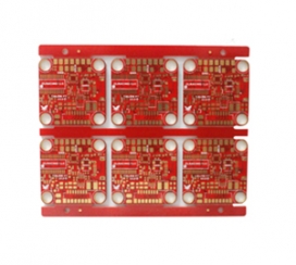
Second, the common layer structures of printed circuit boards include three types: Single Layer PCB , Double Layer PCB and Multi Layer PCB. A brief description of these three layer structures as follows:
(1) Single-layer board: that is, a circuit board with copper on one side and no copper on the other side. Usually components are placed on the side without copper, and the copper side is mainly used for wiring and soldering.
(2) Double-layer board: that is, a circuit board with copper on both sides, usually called one side is the top layer (Top Layer), and the other side is the bottom layer (Bottom Layer). Generally, the top layer is used as the component placement surface, and the bottom layer is used as the component welding surface.
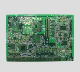
(3) Multilayer board: that is, a circuit board containing multiple working layers. In addition to the top layer and the bottom layer, it also contains several intermediate layers. Usually, the intermediate layer can be used as a wire layer, a signal layer, a power layer, and a ground layer. The layers are insulated from each other, and the connection between layers is usually achieved through vias.
Third, the printed circuit board includes many types of working layers, such as signal layer, protective layer, silk screen layer, internal layer, etc. The functions of various layers are briefly introduced as follows:
(1) Signal layer: mainly used to place components or wiring. Protel DXP usually contains 30 middle layers, namely Mid Layer1~Mid Layer30, the middle layer is used to arrange signal lines, and the top and bottom layers are used to place components or copper.
(2) Protective layer: It is mainly used to ensure that the places on the circuit board that do not need tin plating are not tinned, so as to ensure the reliability of the operation of the circuit board. Among them, Top Paste and Bottom Paste are the top solder mask layer and bottom solder mask layer respectively; Top Solder and Bottom Solder are the solder paste protection layer and the bottom solder paste protection layer respectively. (3) Silk screen layer: It is mainly used to print the serial number, production number, company name, etc. of the components on the printed circuit board.
(4) Internal layer: mainly used as a signal wiring layer, Protel DXP contains a total of 16 internal layers. (5) Other layers: mainly include 4 types of layers.
(5) Other layers: mainly include 4 types of layers.
Drill Guide (drilling orientation layer): mainly used for the location of drilling holes on the printed circuit board.

Mob: 13570819121
Email: txspcbsc@163.com
Web : www.txspcb.cn
Add: Jinkang, No. 1 Shajing Road, Baoan District, Shenzhen
3rd Floor, Building 3, Industrial Park

SWEEP
 Online Service


 中文
中文 English