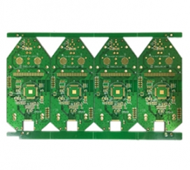
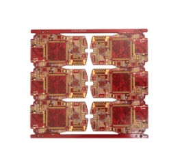
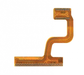
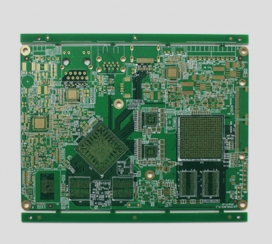
Shenzhen Tengxingsheng Electronics Co., Ltd.
Contact: Miss Wen
Tel: 0755-23286182
Mob: 13570819121
QQ: 1456258664
QQ: 2316907424
Fax: 0755-23286183
Email: txspcbsc@163.com txspcb@163.com
Web : en.txspcb.cn
Add: 3rd Floor, Building 3, Jinkang Industrial Park, No. 1 Shajing Road, Baoan District, Shenzhen
The copper wire of the PCB falls off (also known as copper rejection) is not good. The PCB factory all says that it is the problem of the laminate, and its production factory is required to bear the bad loss. According to my years of experience in handling customer complaints, the common reasons for copper rejection in PCB factories are as follows:
1. Process factors of PCB factory:
1. The copper foil is over-etched. The electrolytic copper foil used in the market is generally single-sided galvanized (commonly known as ashing foil) and single-sided copper-plated (commonly known as reddish foil). For galvanized copper foil above 70um, red foil and ashing foil below 18um basically do not have batch copper rejection.
When the customer's circuit is designed to pass the etching line, if the copper foil specification is changed but the etching parameters remain unchanged, the copper foil will stay in the etching solution for too long. Because zinc is an active metal, when the copper wire on the PCB is immersed in the etching solution for a long time, it will inevitably lead to excessive side etching of the circuit, causing the backing zinc layer of some thin circuits to be completely reacted and separated from the substrate. That is, the copper wire falls off.
Another situation is that there is no problem with the PCB etching parameters, but the washing and drying after etching are not good, causing the copper wire to be surrounded by the etching solution left on the PCB surface. Dump copper. This situation is generally concentrated on thin lines, or during humid weather, similar defects will appear on the entire PCB. Strip the copper wire to see that the color of its contact surface with the base layer (the so-called roughened surface) has changed. The color of the copper foil is different from that of the normal copper foil. The original copper color of the bottom layer is seen, and the peeling strength of the copper foil at the thick circuit is also normal.
2. A local collision occurs in the PCB process, and the copper wire is separated from the substrate by external mechanical force. This defect is manifested as poor positioning or orientation, and there will be obvious twists in the dropped copper wire, or scratches/impact marks in the same direction. Peel off the bad copper wire and look at the rough surface of the copper foil. It can be seen that the color of the rough surface of the copper foil is normal, there will be no bad side corrosion, and the peeling strength of the copper foil is normal.
3. The PCB circuit design is unreasonable. Designing too thin circuits with thick copper foil will also cause excessive circuit etching and copper rejection.
2. Reasons for the laminate process:
Under normal circumstances, as long as the laminate is hot-pressed for more than 30 minutes in the high temperature section, the copper foil and the prepreg are basically completely combined, so the lamination generally does not affect the copper foil and the substrate in the laminate. Binding force. However, in the process of stacking and stacking laminates, if PP is contaminated or the rough surface of the copper foil is damaged, it will also lead to insufficient bonding force between the copper foil and the substrate after lamination, resulting in positioning (only for large boards). language) or sporadic copper wires fall off, but there is no abnormality in the peeling strength of copper foil near the off-wire.
3. Reasons for raw materials of laminates:
1. As mentioned above, ordinary electrolytic copper foils are all galvanized or copper-plated wool foils. If it is not good, the peeling strength of the copper foil itself is not enough. When the bad foil pressed sheet is made into PCB and inserted in the electronic factory, the copper wire will fall off under the impact of external force. This kind of poor copper rejection will not cause obvious side etching after peeling the copper wire to see that the rough surface of the copper foil (that is, the surface in contact with the substrate), but the peeling strength of the copper foil on the whole surface will be very poor.
2. Poor adaptability of copper foil and resin: Some laminates with special properties, such as HTg sheets, are currently used because of different resin systems. The curing agent used is generally PN resin, and the resin molecular chain structure is simple. When curing The degree of crosslinking is low, and it is necessary to use copper foil with special peaks to match it. When producing laminates, the use of copper foil does not match the resin system, resulting in insufficient peel strength of the metal-clad sheet metal foil, and poor copper wire falling off when inserting.

Mob: 13570819121
Email: txspcbsc@163.com
Web : www.txspcb.cn
Add: Jinkang, No. 1 Shajing Road, Baoan District, Shenzhen
3rd Floor, Building 3, Industrial Park

SWEEP
 Online Service


 中文
中文 English