Shenzhen Tengxingsheng Electronics Co., Ltd.
Contact: Miss Wen
Tel: 0755-23286182
Mob: 13570819121
QQ: 1456258664
QQ: 2316907424
Fax: 0755-23286183
Email: txspcbsc@163.com txspcb@163.com
Web : en.txspcb.cn
Add: 3rd Floor, Building 3, Jinkang Industrial Park, No. 1 Shajing Road, Baoan District, Shenzhen
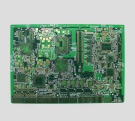
Generally speaking, the more complex the functions of electronic products, the longer the circuit distance and the more contact pins, the more layers the PCB needs. The production process of PCB is relatively complex, and it involves a wide range of processes, from simple machining to complex machining, common chemical reactions, photochemical electrochemical thermochemistry and other processes, computer-aided design CAM and other knowledge. . Moreover, there are many process problems in the production process, and new problems will be encountered from time to time, and some problems will disappear without finding out the cause. Because the production process is a discontinuous assembly line form, any problem in any link will cause the entire line to stop production. Or the consequences of a large number of scrapped , if the printed circuit board is scrapped, it cannot be recycled and reused, and the work pressure of process engineers is high, so many engineers leave this industry and turn to printed circuit board equipment or material suppliers to do sales and technical services. .
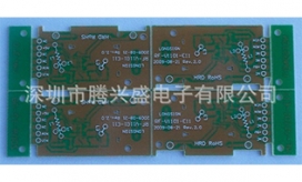
The substrate of the board itself is made of insulating material that is not easy to bend. The thin circuit material that can be seen on the surface is copper foil. After being etched away, the remaining part becomes a mesh of fine lines. These lines are called conductor patterns or wiring, and are used to provide circuit connections for components on the PCB.
In order to fix the parts on the PCB, we solder their pins directly on the wiring. On a basic Z PCB (single-sided), the parts are all concentrated on one side, and the wires are all concentrated on the other side. In this way, we It is necessary to punch holes on the board so that the pins can pass through the board to the other side, so the pins of the parts are soldered on the other side. Because of this, the front and back sides of the PCB are called the Component Side and Solder Side.
If there are some parts on the PCB that need to be removed or put back after the production is completed, the socket will be used when installing the parts. Since the socket is directly welded to the board, the parts can be disassembled and assembled arbitrarily. .
If we want to connect two PCBs to each other, we usually use edge connectors commonly known as "gold fingers". The gold fingers contain many exposed copper pads, which are actually part of the PCB wiring. . Usually when connecting, we insert the gold fingers on one of the PCBs into the appropriate slots on the other PCB (usually called expansion slots). In the computer, such as graphics cards, sound cards or other similar interface cards , are connected to the motherboard by gold fingers.
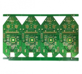
The green or brown on the PCB is the color of the solder mask. This layer is an insulating protective layer that protects the copper wires and prevents parts from being soldered to incorrect places. On the solder mask, there is another A layer of silk screen will be printed. Usually, text and symbols (mostly white) will be printed on this to indicate the position of each part on the board. The silk screen is also called Icon face (legend).
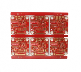
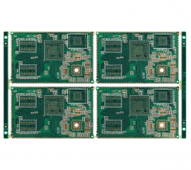
After careful and neat planning, the printed circuit board is etched on a board to provide the main support for electronic components during installation and interconnection. It is indispensable for all electronic products. base parts.
A printed circuit board is a flat plate made of non-conductive material, usually with pre-drilled holes designed to mount chips and other electronic components. The holes of the components help to connect the pre-defined metal paths printed on the board surface electronically. After the pins of the electronic components are passed through the PCB, the conductive metal electrodes are attached to the PCB to form a circuit.

Mob: 13570819121
Email: txspcbsc@163.com
Web : www.txspcb.cn
Add: Jinkang, No. 1 Shajing Road, Baoan District, Shenzhen
3rd Floor, Building 3, Industrial Park

SWEEP
 Online Service


 中文
中文 English